
Usually, to reduce the impurity content in the device region the internal or in situ gettering (IG) technique is applied. IG is provided by bulk SiOx precipitates. In particular, for each SiOx particle formed during precipitation, some Si self-interstitials are produced, due to volume expansion. The so-emitted self-interstitials can form dislocation loops, which usually contain an extrinsic stacking fault. The dislocation loops and the strain field surrounding the precipitates provide the IG.
In the surface region the situation is quite different. Indeed, during annealing oxygen diffuses out from the bulk leaving an oxygen-depleted zone close to the surface, called the denuded zone (DZ). Out-diffusion reduces the interstitial oxygen concentration and then the chemical driving force for oxygen precipitation. As the degree of supersaturation falls the precipitation rate is drastically reduced, reaching zero near the surface region. As a consequence, in this region the defects caused by oxygen precipitation are strongly reduced.
DZ formation and IG are the main procedures used in IC industry to increase device yield.
A very simple model which explains the effect of internal gettering is based on a solution of the one-dimensional diffusion equation. However, oxygen precipitation takes place simultaneously with diffusion since these two processes are indissolubly linked.
We assume that the nucleation centers are uniformly distributed throughout the wafer. Solving proposed system of equations numerically, we calculate the distribution of oxygen with depth in the sample after annealing as a function of time t for any temperature.
The concentration profiles allow us to estimate the denuded zone width (DZW) which is obtained as a result of annealing. As a criterion of our estimate of the DZW from the calculated concentration profiles, we chose a quantity proportional to the dispersion of the concentration profile.
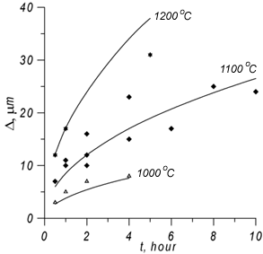
Fig.3. Denuded zone width as a function of first annealing temperature and time.
Results of this estimate are compared in Fig.3 with experimental data. Despite the large error in the experimental determination of the DZW (this quantity is determined from the results of microscopic observations of a cleavage face of the wafer after selective etching) and the uncertainty in the criterion, we find the agreement to be satisfactory.
| Main page | Research interests | Stuff and contact information | Publications |